
The new large-die device, which hits 90 mΩ on-resistance and 55 A drain current, is currently sampling to U.S. customers. By leveraging a junction-barrier Schottky FET (JBSFET) construction, the design aims to mitigate body diode degradation, a common failure point in high-stress environments. These components are intended for heavy-duty applications, including rail traction, MW-scale EV charging, and solid-state transformers.
NoMIS Power Hits 8 kV Milestone in High-Voltage SiC Roadmap
Albany-based NoMIS Power has successfully demonstrated its first 6.5 kV silicon carbide MOSFET, achieving over 8 kV of blocking capability. This performance milestone marks a shift for the U.S. manufacturer, validating its planar technology as it prepares to scale production toward 10 kV MOSFETs and 20 kV SiC IGBTs.
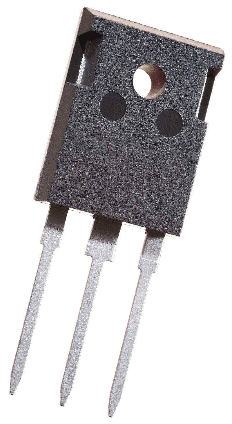
Dr. Adam Morgan, CEO of NoMIS Power, noted that the successful scaling from the company’s existing 3.3 kV line to this high-voltage class establishes a domestic supply chain for sectors like aerospace and defense. With standard production for the 6.5 kV line slated for Q4 2026, the company is positioning itself as a secure alternative to foreign single-source dependencies. Operating out of the Albany Nanotech Complex, NoMIS Power is currently engaging developers to integrate these high-voltage solutions into government-funded programs, with plans to push their architecture toward the 20 kV threshold in the coming years.




Comments (0)
No comments yet. Be the first!