
The new facility, located in Phase III of the Batu Berendam Free Trade Zone, will specialize in the production of high-end Embossed Carrier Tapes and Cover Tapes. By localizing manufacturing, the company aims to reduce lead times for OSAT and semiconductor customers while providing high-precision packaging interfaces suited for chip miniaturization and Chiplet integration. Mass production is slated to begin early next year, following the current phase of sample testing and qualification.
E&R Engineering Expands Semiconductor Packaging to Malaysia
E&R Engineering will inaugurate its new Malaysian subsidiary, E&R SEMICONDUCTOR (MALAYSIA) SDN. BHD., at the Melaka Free Trade Zone on October 13. This strategic expansion signals a shift in production focus as the company moves to capitalize on the region’s growing semiconductor backend packaging and testing sector.
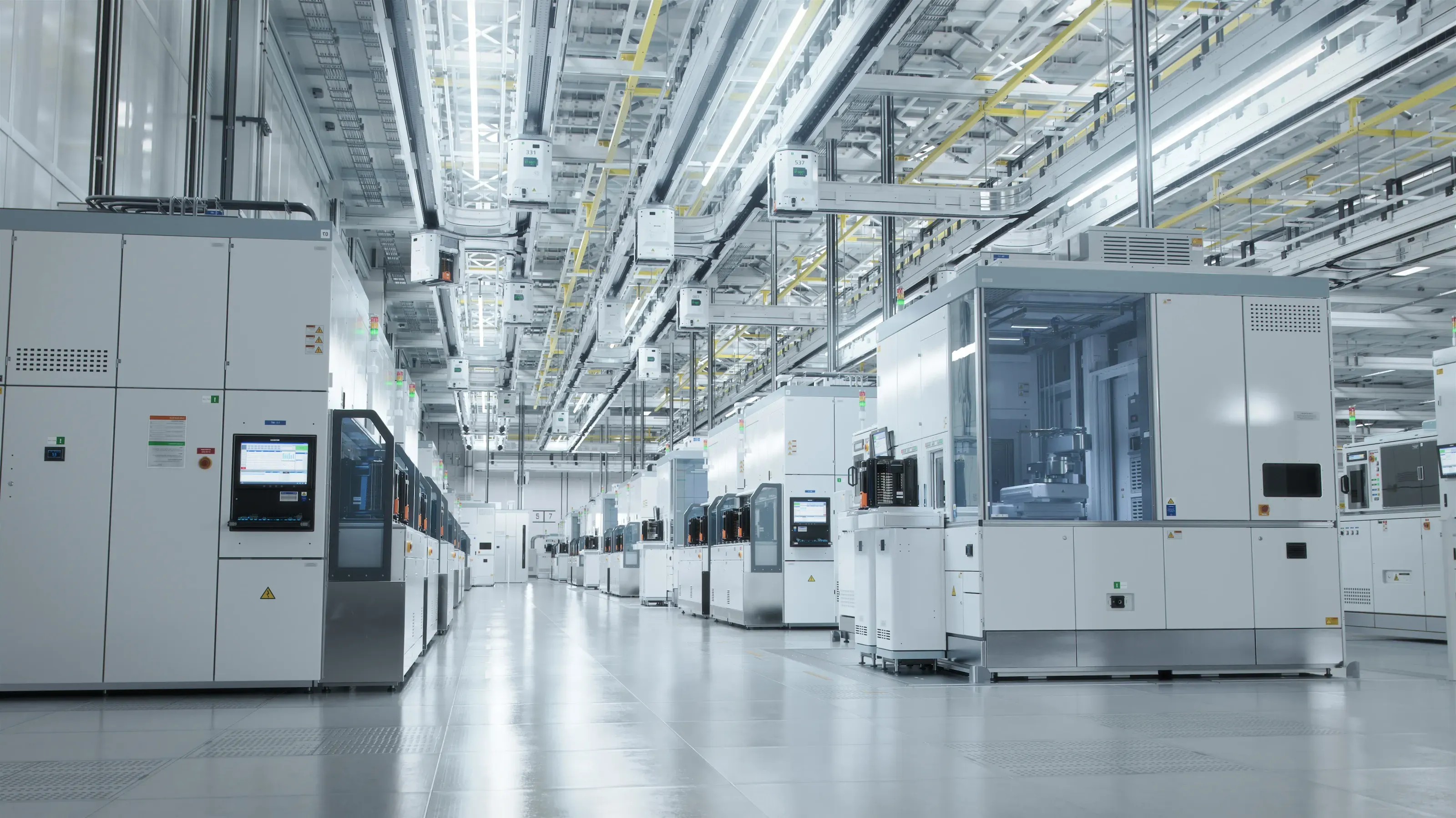
Beyond manufacturing, the site will function as a hub for Field Service Engineers to provide immediate technical support to regional clients. The company expects the plant to generate 50 local jobs while strengthening its supply chain capabilities. President KS Chen noted that this move addresses surging Southeast Asian demand, allowing for a more agile response to the needs of local semiconductor manufacturers. General Manager AK Ong emphasized that the proximity to customers will allow the company to maintain rigorous quality control while delivering real-time after-sales services.



Comments (0)
No comments yet. Be the first!